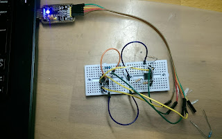
Reverse engineering an AKD2001
Per previous post, my unusal/1st gen AKD
Some notes:
Processor: MC6802
PLL NJ88C30, PLL Reference Oscillator 10MHz, Ref Osc divisor = 400, channel spacing = 25KHz
On RX VCO runs at RX Frequency - 1st IF (10.7MHz)
TX VCO runs at TX Frequency.
EPROM 27C128 Mapped to $E000-$FFFF (mostly unused, No code before FC00, only 1K used)
It seems to be a very simple design where the various 'peripheral' parts are memory mapped using a 74LS138 3-8 Decoder, it's not fully decoded so any write which addresses A13, A14, A15 or any combination will enable an output on the 'LS138

CP is the clock pulse for the 4024 Binary counter which generates the 1750 Toneburst
CLK is the PLL Clock
Latch is the PLL Latch signal
FPSEL and FP14 are related to the front panel, not sure how that works yet
OE is the EPROM Select
And some NOR logic:

'FP' signals are related to the front panel, the front panel connector:

Amazingly, the entire operating code for the radio takes only 336 bytes!
I don't think I could even persuade a modern processor to start up in that few bytes.
Memory map of EPROM:
Reset Vector at $FFFE-$FFFF is $FC00 and yes, the code begins at $FC00
IRQ Vector is $FC71 and there's an IRQ handler routine there.
IRQ seems to be from the front panel, suspect it's generated on keypress
Channel table seems to start at $FE00-$FFC7
The entire channel table:
0F 00 16 A8 15 14
1F 10 16 A9 15 15
2F 20 16 AA 15 16
3F 30 16 AB 15 17
4F 40 16 AC 15 18
5F 50 16 AD 15 19
6F 60 16 AE 15 1A
7F 70 16 AF 15 1B
00 80 16 B0 15 04
00 90 16 B1 15 05
00 01 16 B2 15 06
00 11 16 B3 15 07
00 21 16 B4 15 08
00 31 16 B5 15 09
00 41 16 B6 15 0A
00 51 16 B7 15 0B
00 61 16 B8 15 0C
00 71 16 B9 15 0D
00 81 16 BA 15 0E
00 91 16 BB 15 0F
00 02 16 BC 15 10
00 12 16 BD 15 11
00 22 16 BE 15 12
00 32 16 BF 15 13
00 42 16 94 14 E8
00 52 16 95 14 E9
00 62 16 96 14 EA
00 72 16 97 14 EB
00 82 16 98 14 EC
00 92 16 99 14 ED
00 03 16 9A 14 EE
00 13 16 9B 14 EF
00 23 16 9C 14 F0
00 33 16 9D 14 F1
00 43 16 9E 14 F2
00 53 16 9F 14 F3
00 63 16 A0 14 F4
00 73 16 A1 14 F5
00 83 16 A2 14 F6
00 93 16 A3 14 F7
00 04 16 A4 14 F8
00 14 16 A5 14 F9
00 24 16 A6 14 FA
00 34 16 A7 14 FB
00 44 16 C8 15 1C
00 54 16 C9 15 1D
00 64 16 CA 15 1E
00 74 16 CB 15 1F
00 84 16 CC 15 20
00 94 16 CD 15 21
00 05 16 CE 15 22
00 15 16 CF 15 23
00 06 16 A8 14 FC
00 16 16 A9 14 FD
00 26 16 AA 14 FE
00 36 16 AB 14 FF
00 46 16 AC 15 00
00 56 16 AD 15 01
00 66 16 AE 15 02
00 76 16 AF 15 03
00 07 16 C0 15 14
00 17 16 C1 15 15
00 27 16 C2 15 16
00 37 16 C3 15 17
00 47 16 C4 15 18
00 57 16 C5 15 19
00 67 16 C6 15 1A
00 77 16 C7 15 1B
00 09 16 C0 14 FC
00 19 16 C1 14 FD
00 29 16 C2 14 FE
00 39 16 C3 14 FF
00 49 16 C4 15 00
00 59 16 C5 15 01
00 69 16 C6 15 02
00 79 16 C7 15 03
Each channel seems to be 6 bytes of data,
First channel:
"0F 00 16 A8 15 14"
0F, not sure yet but the first byte only appears on repeater channels where the tone burst can be enabled.
00, The channel number for display on the LEDs
16 A8 is the TX VCO divisor
15 14 is the RX VCO divisor
Our Reference frequency is 25KHz
TX Divisor $16 $A8 equals 5800 Decimal,
5800 * .025 = 145MHz
RX Divisor $15 $14 = 5396
Same as before, 5396 * .025 = 134.9MHz
RX Frequency = RX VCO + 10.7MHz IF = 145.6
So the first channel is set up as a repeater,
The 4024 chip in the radio seems to be a 1750Hz Toneburst generator, pretty useless these days but it must be switched on or off, not sure if it's in the EPROM or not, yet.
More later.


Comments
Post a Comment